ZEISS EVO Family
Advanced SEM System for User-friendly Operation, Regular Assessments, and Diverse Research
EVO's tools blend top-tier SEM with ease of use, suitable for experts and novices. Customizable for diverse scientific needs, it's ideal for life and material sciences or standard industrial checks and breakdown analysis.
- A multipurpose choice for core microscopy labs or industrial QA.
- Superior imaging for real samples.
- Optimal visuals via the LaB6 emitter.
- Superior imaging and analysis on non-coated, non-conductive materials.
- Streamlined processes and data accuracy
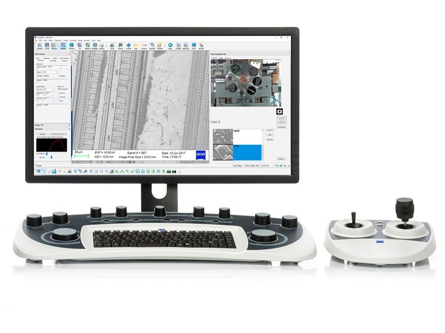
World Class User Experience
SmartSEM Touch offers direct, interactive control over workflows. Its learning curve is notably short, significantly cutting down training time and expense. Novices can start obtaining impressive visuals within minutes. Furthermore, its interface caters to industrial professionals needing consistent, automated inspection procedures
Hightlights
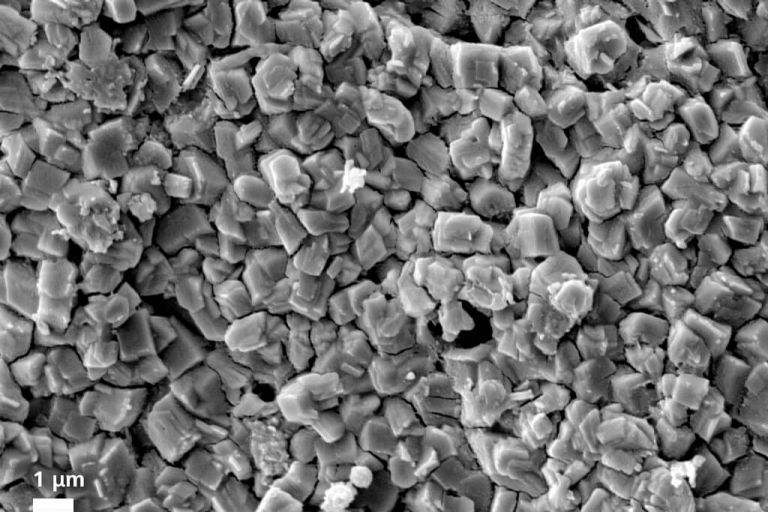
Outstanding Image Clarity
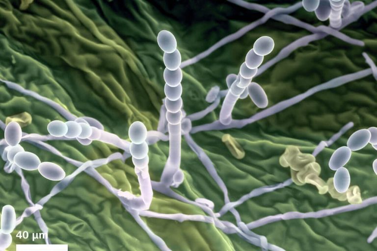
EVO adeptly maximizes data clarity from untouched, uncoated specimens. It also maintains the integrity of data for moist and highly contaminated samples by preserving their original state. Moreover, the LaB6 emitter enhances resolution, contrast, and signal-to-noise, crucial during demanding imaging and microanalysis.
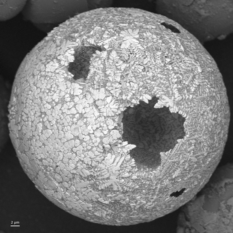
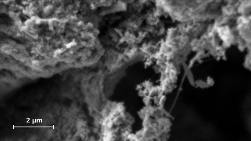
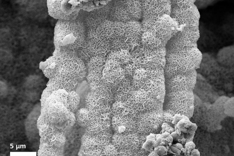
Caption: Flint, particle of ferrocerium from a fire starter, captured with ZEISS EVO, HDBSD detector
EVO Integrates Seamlessly
EVO can be tailored for semi-automated multi-modal processes, offering tools for effortlessly pinpointing areas of interest and maintaining data integrity across varied modalities. Merge data from both light and electron microscopes for material assessment or component inspection. Pair EVO with ZEISS light microscopes for comparative particle analysis
Broadening Accessibility
While SEM operation might traditionally be reserved for expert electron microscopists, often there's a need for non-experts, like students or quality engineers, to access SEM data. EVO addresses this by offering user interfaces tailored for both seasoned microscopists and novices.
Utilizatorii experți beneficiază de interfața SmartSEM, accesând parametri de imagistică sofisticați și capacități de analiză detaliată
Utilizatorii novici navighează cu SmartSEM Touch, accesând fluxuri de lucru prestabilite și parametrii frecvent utilizați, ideal pentru începători

Smart Imaging and Navigation
Enhance your sample processing, efficiency, and outcomes
Sistemul de cameră de navigație ZEISS
Atașați o cameră la cameră pentru a monitoriza pozițiile probelor în raport cu detectorul retrodifuzat sau pe ușa camerei pentru o vedere aeriană, simplificând navigația și configurarea locației probelor.
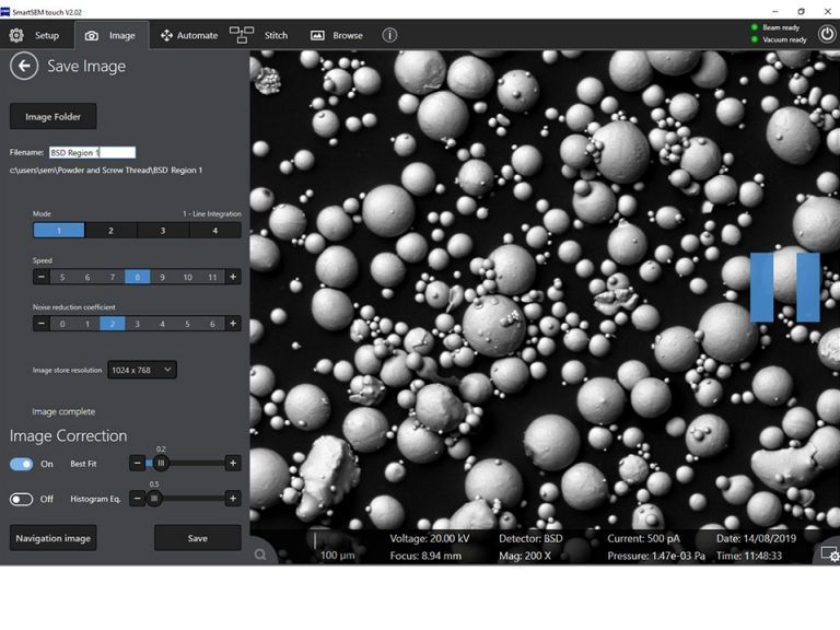
Automated Smart Imaging with EVO
EVO offers unattended, automatic image acquisition for sample batches. ZEISS's Automated Smart Imaging is ideal for routine checks, allowing users to define boundaries, generate areas of interest based on magnification, and start automated captures. Enhance your sample processing rate and optimize productivity
Optimized Imaging with LaB6 Electron Emitter
Using a lanthanum hexaboride cathode over traditional tungsten ensures superior image quality. This offers dual benefits:
- With similar electron probe sizes, image navigation and optimization are simpler.
- For equal probe currents, the beam is finer, improving resolution.
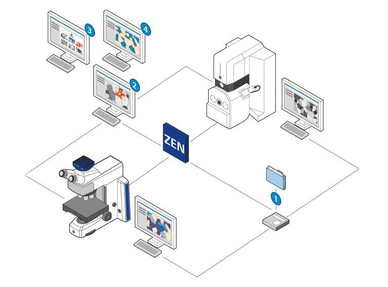
Extend Potential with ZEISS ZEN core
The Ultimate Software for Integrated Microscopy & Analysis ZEISS, a leading microscopy and metrology provider, ensures EVO seamlessly integrates with its range. Enhance productivity by connecting digital light microscopes and EVO. Leverage the distinct contrasts from light microscopes and SEM's unique imaging to gather holistic data on samples.
ZEN core acts as your centralized hub for interconnected microscopy. Tailor it to suit your needs and design workflows respecting the proficiency of all users.
Key features include:
- Correlative Microscopy: Interchange data between different microscope types.
- Data Visualization: Organize and view data across varied scales and modalities.
- Metallography with Word-Integrated Reporting: Unified reports combining images and data.
- AI-driven Image Analysis: Image breakdown using advanced machine learning
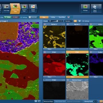
EDX Solutions for In-depth Microanalysis
When SEM imaging falls short of providing comprehensive insights into samples or parts, researchers utilize Energy Dispersive Spectroscopy (EDS) to obtain detailed elemental chemistry data at specific spatial locations
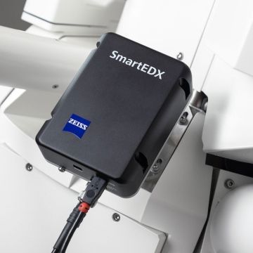
ZEISS SmartEDX - Tailored for Routine Microanalysis
Specially designed for routine microanalysis, SmartEDX on EVO delivers unmatched data reproducibility, highlighting its excellence with a 129 eV energy resolution at 1-5 nA probe current. Enhanced to capture low energy X-rays from light elements, it benefits from the superior transmissivity of the silicon nitride window
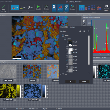
Workflow-Guided Interface of ZEISS SmartEDX
SmartEDX's interface, in line with ZEISS's user-focused approach, ensures ease of learning and intuitive operation. It promotes consistent analytical task execution on the SEM, especially in multi-user settings. Whether you're looking for the best cost-performance EDS detector in a fixed configuration or a versatile slider version, SmartEDX offers both
Streamlined Operation for Efficient EDS Data Gathering
Simultaneously manage both EDS and SEM through a unified PC interface, enhancing user experience. Benefit from specialized user interfaces for both your microscope and EDS system. Exploit the integrated detector optimization to slash EDS collection time, amplifying the EDS signal input by a minimum of 17%.
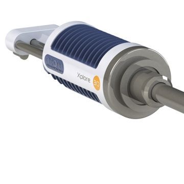
Diverse EDX Detector Options at Your Disposal
A unified PC solution presents an array of EDS configurations. Options such as the Xplore 15, 30, and the Ultim Max 40 detectors from Oxford Instruments are available for selection
Comprehensive ZEISS Support and Service for the Entire System
With SmartEDX wholly backed by ZEISS, it becomes the perfect EDS solution for those seeking to simplify their analytical equipment suppliers. ZEISS manages every aspect - from installation, preventive maintenance, warranty claims, diagnostics, repairs, spare parts logistics, to comprehensive system service contracts. This ensures a seamless support experience for your analytical SEM solution
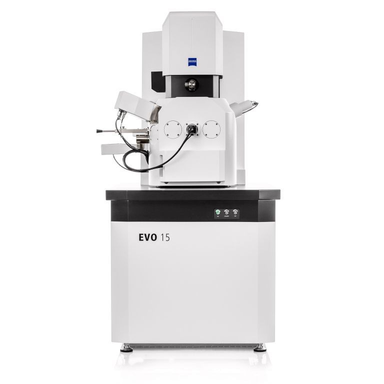
The EVO Family
| ZEISS EVO 10 | ZEISS EVO 15 | ZEISS EVO 25 | |
|---|---|---|---|
| Choose EVO 10—with optional backscatter detector and Element EDS system—to be your entry point to scanning electron microscopy, at a remarkably affordable price. Even this smallest of EVO vacuum chambers is well differentiated from tabletop SEMs. Your investment in EVO now assures that you are ready for applications that require more space and ports than you anticipate today. | EVO 15 demonstrates the flexibility concept of the EVO family and excels in analytical applications. Opt for the larger vacuum chamber of the EVO 15, and add variable pressure for imaging and analysis of non-conductive samples or parts, and you have a versatile, multi-purpose solution for central microscopy facilities or industrial quality assurance laboratories. | EVO 25 is the industrial workhorse solution with enough space to accommodate even the largest parts and assemblies. Expand EVO 25 capabilities further with an optional 80 mm Z travel stage that can handle weights up to 2 kg even with tilt. Additionally, the large chamber will accommodate multiple analytical detectors for the most demanding microanalysis applications. | |
| Maximum specimen heights | 100 mm | 145 mm | 210 mm |
| Maximum specimen diameter | 230 mm | 250 mm | 300 mm |
| Motorized stage travel XYZ | 80 x 100 x 35 mm | 125 x 125 x 50 mm | 130 x 130 x 50 (or 80) mm |
| High Vacuum (HV) mode Best quality imaging and analysis on conductive samples |
✓ | ✓ | ✓ |
| Variable Pressure (VP) mode High quality imaging and analysis on uncoated, non-conductive samples |
✓ | ✓ | ✓ |
| Extended Pressure (EP) mode Environmental imaging of hydrated or contaminated samples in their natural state |
✓ | ✓ | ✓ |
Accessories
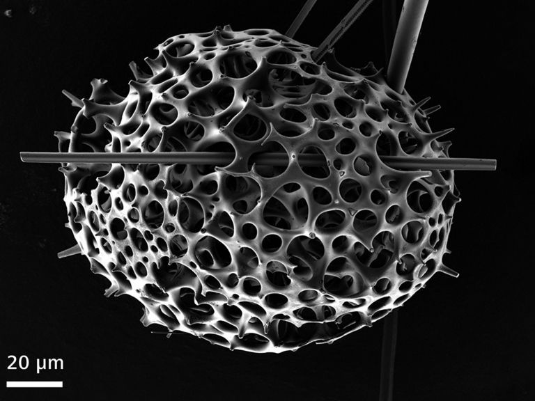
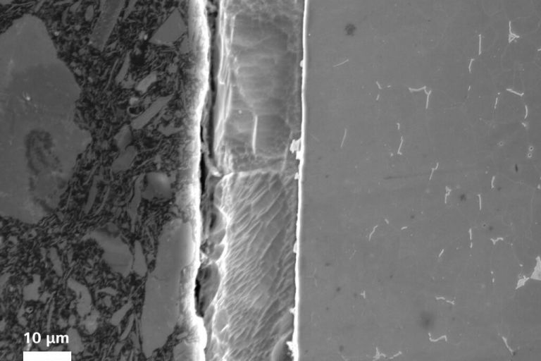
Enhanced Imaging with Beam Deceleration
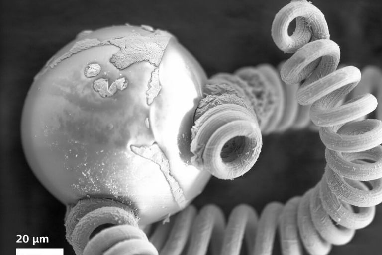
Utilize beam deceleration imaging for examining particularly sensitive specimens. Achieve superior image clarity while reducing specimen damage. Obtain higher resolution, increased surface sensitivity, and enhanced contrast when imaging non-conductive samples. By applying a bias voltage to your specimen, the effective landing energy is reduced, maintaining the primary energy at a high level.
An uncoated Radiolaria alga was observed at 1 keV landing energy. Without beam deceleration, the image exhibits charging artifacts (left). However, with beam deceleration applied, there's a noticeable improvement in surface details and contrast, and a significant reduction in charging artifacts (right).
Applications
Manufacturing & Assembly Industries Applications
- Quality Analysis & Quality Control
- Failure Analysis & Metallography
- Cleanliness Inspection
- Particle Morphological & Chemical Analysis compliant with ISO 16232 and VDA 19 Part 1 & 2 standards
- Non-metallic Inclusions Analysis
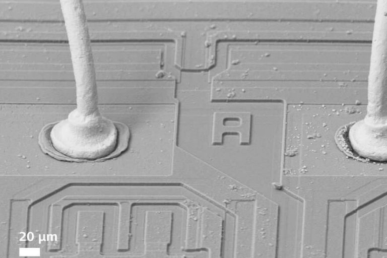
Semiconductors & Electronics Applications
- Visual Inspection: Electronic components, integrated circuits, MEMS devices, solar cells
- Copper Wire: Surface and crystal structure analysis
- Metal Corrosion: Detailed investigations
- Cross-sectional: Failure analysis
- Bonding: Foot inspections
- Capacitors: Surface imaging
Steel and Other Metals Applications
- Imaging & Analysis: Structure, chemistry, and crystallography of metals and inclusions
- Assessments: Phase, particle, weld, and failure analysis
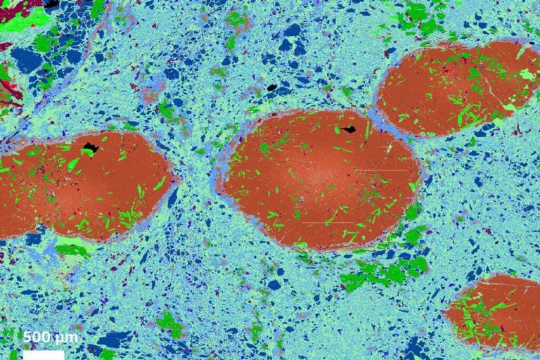
Raw Materials Applications
- Geological Samples: Morphology, mineralogy, and compositional analysis.
- Metals Examination: Imaging and analysis of structure, fractures, and nonmetallic inclusions.
- Chemicals & Ingredients: Morphological and compositional study during micronization and granulation
Materials Science Research
- Analysis of conductive and non-conductive materials for investigative purposes.
Științe biologice
- Explorarea plantelor, animalelor și microorganismelor.
Forensics
- Gunshot residue (GSR) analysis.
- Examination of paint and glass.
- Investigation into banknote and coin forgery.
- Hair and fiber comparisons.
- Forensic toxicology studies
Documents and brochures
 ZEISS EVO
 ZEISS Microscopy Solutions for Steel and Other Metals
 ZEISS SmartEDX
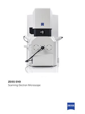 ZEISS Evo
Do You Need Help?
We are here to provide you with all the information and assistance you need regarding our products. Please fill out the contact form below, and we will promptly answer your questions or provide you with the support you need to make the right decisions.
News and events
Join the most important events and stay up to date with the latest industry news

Forumul de Inovație ZEISS & Marea Deschidere INMAACRO Timișoara I 19.03.2026
Avem plăcerea de a vă invita la evenimentul de inaugurare a noului laborator de măsurări din Timișoara, unde vă vom prezenta soluții pentru controlul calității, pe 19 Martie, începând cu ora 09:30. Experimentați universul metrologiei în cadrul unei expoziții interesante și prin prezentări interactive!

Ziua Calității ZEISS 2025 | 06.11.2025
Pe 6 Noiembrie, pregatiți-vă pentru un workshop exclusiv dedicat profesioniștilor în controlul calității. Descoperiți soluții concrete pentru provocările din producție, participați la demonstrații live cu echipamente de ultimă generație și beneficiați de consultanță personalizată pentru a vă optimiza procesele de măsurare.

Technical News in Turning and Grinding – WORKSHOP | 08.05.2025
We invite you to an event dedicated to the latest technical solutions in the field of turning and grinding! Together with our top partners – BRUCKNER, BLOHM JUNG, INDEX, STUDER, WALTER EWAG – you will explore the most advanced technologies and attend live demonstrations that will address the needs and challenges you face in your activity.

Ziua Calității ZEISS 2024 | 21 Noiembrie 2024
Vă invităm la un nou eveniment anual exclusiv în care vom prezenta pentru a treia oară soluții de asigurare a calității împreună cu partenerul nostru ZEISS. Explorați împreună cu noi lumea metrologiei industriale ZEISS..